

PCB Layout
Comprehensive routing capabilities
DipTrace PCB Layout is a professional, constraint-driven board design environment for engineering teams working on dense multilayer boards with high-speed and mixed-signal requirements. The design rule system is built on net classes, class-to-class clearances and per-object settings for every class and layer, and real-time DRC validates each action against those rules before it is committed to the board. Interactive routing with push and shove, interactive editing, differential pair routing with phase and length tolerance, length matching and a shape-based autorouter cover the full routing workflow, while electrical and physical parameters are calculated for traces, transmission lines, differential pairs and planar inductors. Layer stackup, via styles and blind and buried vias are managed per project. Boards are verified against the source schematic, previewed in hardware-accelerated 3D, exported for mechanical CAD, and released to manufacturing in Gerber X2, ODB++ and IPC-2581C.

PCB Layout provides the
following features

Smart project structure
DipTrace is a single environment with direct circuit-to-board converting, updating from schematic or netlist, back annotation, real-time cross highlight and selection. Nets are divided into net classes with custom settings and class-to-class rules. Through and blind/buried vias are organized to via styles.

Placement features
Components can be placed manually by simple drag & drop, special "Placement by list" and "Cross selection from schematic" features; or automatically according to custom settings and with optimized length of traces. For excellent results use a combination of all available placement methods.

Interactive routing
Push-and-shove routing at 90/45 or free angles, with arcs and curves, several route and edit modes, automatic via placement and trace parameters changed on the fly. Routing holds net class and class-to-class rules. Shape-based copper pour, configurable via stitching and via shielding, teardrops for pads, vias, trace width changes and T-junctions.
Interactive editing
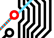
Move traces, vias, components, pads, mounting holes, shapes or the board outline while surrounding traces and vias make room automatically. Edited traces walk around pads and keepouts, and redundant traces are removed on reroute. Editing enforces design rules continuously or returns objects to the last violation-free position.
Smart project structure
DipTrace is a single environment with direct circuit-to-board converting, updating from schematic or netlist, back annotation, real-time cross highlight and selection. Nets are divided into net classes with custom settings and class-to-class rules. Through and blind/buried vias are organized to via styles.
Placement features
Components can be placed manually by simple drag & drop, special "Placement by list" and "Cross selection from schematic" features; or automatically according to custom settings and with optimized length of traces. For excellent results use a combination of all available placement methods.
Interactive routing
Push-and-shove routing at 90/45 or free angles, with arcs and curves, several route and edit modes, automatic via placement and trace parameters changed on the fly. Routing holds net class and class-to-class rules. Shape-based copper pour, configurable via stitching and via shielding, teardrops for pads, vias, trace width changes and T-junctions.
Interactive editing
Move traces, vias, components, pads, mounting holes, shapes or the board outline while surrounding traces and vias make room automatically. Edited traces walk around pads and keepouts, and redundant traces are removed on reroute. Editing enforces design rules continuously or returns objects to the last violation-free position.
High-speed autorouter
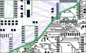
DipTrace high-class shape-based autorouter with advanced settings is capable of routing complex multi-layer boards, as well as simple single-layer boards with jumper wires. DSN/SES interface provides support for external routers (Specctra, Electra, Topor etc.).

High-speed and differential signaling
Comprehensive length-matching capabilities - real-time length comparison table, DRC length-tolerance rules, and meander placement tool - allow the DipTrace user to achieve correct timing for high-speed nets and buses. Differential pairs with advanced phase and length parameters are easy to route with double or single track routing modes. Phase tuning tool allows for precise and fast correcting of phase shifts. The software considers layer stackup and bonding wires when calculating the length of a high-speed net or phase of a differential pair.

Advanced verification features
DipTrace provides an error-free design environment. DRC verifies clearances between design objects, size limits, and differential pair phase/length constraints. Rules are defined by object types, layers, net classes, and class-to-class settings. Real-time DRC checks every action and shows errors before actually making them. Net Connectivity guarantees that all nets have been properly routed and reports broken and merged nets. Comparing to schematic allows the designer to find differences between the PCB and the source schematic.
High-speed autorouter
DipTrace high-class shape-based autorouter with advanced settings is capable of routing complex multi-layer boards, as well as simple single-layer boards with jumper wires. DSN/SES interface provides support for external routers (Specctra, Electra, Topor etc.).
High-speed and differential signaling
Comprehensive length-matching capabilities - real-time length comparison table, DRC length-tolerance rules, and meander placement tool - allow the DipTrace user to achieve correct timing for high-speed nets and buses. Differential pairs with advanced phase and length parameters are easy to route with double or single track routing modes. Phase tuning tool allows for precise and fast correcting of phase shifts. The software considers layer stackup and bonding wires when calculating the length of a high-speed net or phase of a differential pair.
Advanced verification features
DipTrace provides an error-free design environment. DRC verifies clearances between design objects, size limits, and differential pair phase/length constraints. Rules are defined by object types, layers, net classes, and class-to-class settings. Real-time DRC checks every action and shows errors before actually making them. Net Connectivity guarantees that all nets have been properly routed and reports broken and merged nets. Comparing to schematic allows the designer to find differences between the PCB and the source schematic.
Multithreaded processing
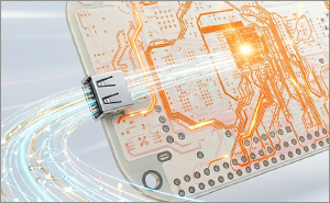
Copper pour filling, design rule checking and net connectivity verification run in multiple threads and scale with the number of available CPU cores. On dense multilayer boards with large pour areas and high net counts, full-board verification stays fast enough to run continuously during layout.

3D PCB preview & STEP export
PCB Layout module includes real-time 3D preview feature with hardware acceleration. It shows a model of the manufactured printed circuit board with all components installed. The board can be rotated on three axes, zoomed in and out; preview colors are customizable. You can export the board to STEP or VRML 2.0 format for mechanical CAD modelling. 3D feature supports *.wrl, *.3ds, *.step, and *.iges 3D component models. More than 11,000 3D models are shipped with the program.
Import / export
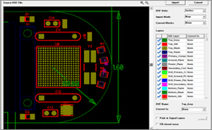
Exchange layouts and libraries with Altium, OrCAD, PADS, P-CAD, Eagle, KiCad and DXF. Import netlists from Accel, Allegro, Mentor, PADS, P-CAD, KiCad, Protel and Tango, and designs from ODB++ and PADS VX ASCII.
Multithreaded processing
Copper pour filling, design rule checking and net connectivity verification run in multiple threads and scale with the number of available CPU cores. On dense multilayer boards with large pour areas and high net counts, full-board verification stays fast enough to run continuously during layout.
3D PCB preview & STEP export
PCB Layout module includes real-time 3D preview feature with hardware acceleration. It shows a model of the manufactured printed circuit board with all components installed. The board can be rotated on three axes, zoomed in and out; preview colors are customizable. You can export the board to STEP or VRML 2.0 format for mechanical CAD modelling. 3D feature supports *.wrl, *.3ds, *.step, and *.iges 3D component models. More than 11,000 3D models are shipped with the program.
Import / export
Exchange layouts and libraries with Altium, OrCAD, PADS, P-CAD, Eagle, KiCad and DXF. Import netlists from Accel, Allegro, Mentor, PADS, P-CAD, KiCad, Protel and Tango, and designs from ODB++ and PADS VX ASCII.
Native XML for Git workflows
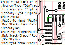
Projects are stored in native XML, a text-based format suitable for Git, Mercurial and other external version control systems. Copper pour data is written compressed or as plain text. Version control is provided by the repository, not by DipTrace.

Manufacturing output
Gerber RS-274X and Gerber X2, Excellon N/C drill, ODB++, IPC-2581C, IPC-D-356A netlist, pick and place, BOM and DXF. Vector and TrueType font export. Milling method support. DipTrace is a listed ODB++Design development partner.
Native XML for Git workflows
Projects are stored in native XML, a text-based format suitable for Git, Mercurial and other external version control systems. Copper pour data is written compressed or as plain text. Version control is provided by the repository, not by DipTrace.
Manufacturing output
Gerber RS-274X and Gerber X2, Excellon N/C drill, ODB++, IPC-2581C, IPC-D-356A netlist, pick and place, BOM and DXF. Vector and TrueType font export. Milling method support. DipTrace is a listed ODB++Design development partner.